
Epoxy Encapsulation for PCB Buyer Guide
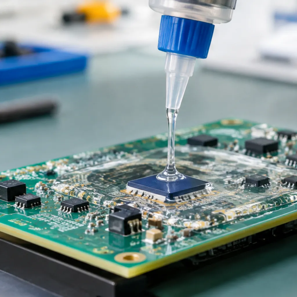
Are you worried that a potting failure might ruin your next electronics build?
Applying epoxy encapsulation for PCB assemblies offers unbeatable protection against moisture, thermal shock, and mechanical stress. But get the process wrong—whether it’s cure shrinkage, trapped air voids, or hidden ionic contamination—and you risk destroying sensitive components before your board ever ships.
In this guide, you’ll discover the exact steps to ensure a flawless potting process: from critical surface preparation and material compatibility to board-level qualification and partnering with RW ATELIER for zero-defect production.
Let’s dive right in.
Quick Answer
Epoxy encapsulation for PCB assemblies—commonly referred to as potting—is a high-reliability process that seals an entire printed circuit board inside a solid, cross-linked polymer compound. This permanent barrier protects sensitive electronic assemblies from moisture ingress, corrosive chemicals, mechanical shock, vibration, and thermal cycling.
Core Protection Benefits at a Glance
- Total Environmental Sealing: Complete protection against liquid submersion, high humidity, dust, and corrosive industrial atmospheres.
- Superior Dielectric Insulation: Outstanding electrical insulation epoxy properties that prevent high-voltage arcing, short circuits, and leakage currents across densely packed traces.
- Mechanical Integrity: Exceptional shock and vibration absorption, locking surface-mount devices (SMDs) and through-hole components securely to the substrate.
- Thermal & Chemical Endurance: High-performance resistance against thermal shock, petroleum fluids, automotive chemicals, and elevated operating temperatures.
- Tamper & IP Protection: An opaque, rigid electronic encapsulant layer conceals proprietary circuit layouts, reverse-engineering attempts, and prevents unauthorized repairs.
| Key Metric | Standard Industry Value | High-Performance Target |
|---|---|---|
| Dielectric Strength | 15–20 kV/mm | >25 kV/mm |
| Operating Temperature | -40°C to +130°C | -60°C to +180°C |
| Moisture Absorption | <0.5% (24h immersion) | <0.1% |
| Cure Shrinkage | 1.0%–2.5% | <0.5% (low-stress) |
When absolute board-level survival is mandatory in automotive, aerospace, marine, or extreme industrial environments, selecting the right PCB potting epoxy formulation ensures failure-free, long-term field operation.
What Buyers Need to Know First
Before committing to an epoxy encapsulation for PCB assembly, you need to understand that this is a permanent decision. Unlike reworkable silicones or thin conformal coatings, cured epoxy creates an impenetrable barrier. Once the electronic encapsulant cures, component repair is practically impossible.
Here are the critical factors we urge buyers to evaluate before ordering bulk materials:
- Thermal Expansion (CTE) Mismatch: The resin and your circuit board expand at different rates under heat. A high-expansion material will tear solder joints clean off the board during thermal cycling.
- Operating Temperature Limits: Standard systems handle daily industrial conditions, but harsh environments demand a dedicated high temperature epoxy resin or specialized cryogenic formulations.
- Viscosity and Flow: Thick compounds struggle to wet beneath fine-pitch BGAs. You need the right flow rate to ensure complete underneath coverage without trapping air.
- Exotherm Control: Epoxy releases heat as it cures. Large volume pours can overheat and fry delicate semiconductors before the system even leaves the factory floor.
| Property to Specify | Why It Matters for Your PCB |
|---|---|
| Glass Transition Temp ($T_g$) | Dictates where the resin shifts from rigid to flexible |
| Dielectric Strength | Guarantees proper electrical insulation epoxy performance |
| Volumetric Shrinkage | Low shrinkage prevents micro-cracking delicate silicon dies |
| Cure Profile | Determines whether room-temp cure or heat cure fits your line |
Choosing the right circuit board encapsulation resin upfront prevents catastrophic field failures, board warpage, and costly production scrap.
PCB Preparation Before Encapsulation
Getting your board ready is the single most critical step before pouring any resin. If the surface isn’t properly prepped, even the highest-grade epoxy encapsulation for PCB assemblies will delaminate, trap moisture, or fail dielectric testing down the road.
We always focus on three mandatory pre-potting checkpoints:
- Moisture Bake-Out: Circuit boards and surface-mount devices absorb ambient moisture. We recommend baking boards at 80°C to 100°C for at least 2 to 4 hours before dispensing to eliminate outgassing during the cure cycle.
- Surface Energy Activation: Low surface energy plastics (such as Teflon or untreated polyolefin connectors) resist bonding. Plasma or corona treatment raises surface energy, giving the PCB potting epoxy a clean, anchor-ready profile.
- Physical Masking: Protect test points, connectors, switches, and tuning screws. Use high-temperature silicone-free tapes or custom boots to prevent the electronic encapsulant from creeping into contact areas via capillary action.
Compatibility with Components and Coatings
A successful circuit board encapsulation project requires complete chemical harmony between the liquid resin and your assembled hardware. When raw chemistry clashes with your bill of materials, you risk incomplete curing, corrosion, or stress cracking.
| Board Element | Potential Risk | Engineering Fix |
|---|---|---|
| Solder Mask | Poor adhesion or interfacial lifting | Validate mask surface tension; avoid gloss finishes that prevent mechanical interlocking with the PCB protection resin. |
| No-Clean Flux Residue | Inhibits cure kinetics; promotes dendrite growth | Clean thoroughly with saponified washes or select a chemically tolerant custom epoxy formulation. |
| Silicone Traces | Total loss of adhesion (fish-eyes) | Strictly isolate silicone greases or conformal coatings from the epoxy potting line. |
| Sensors & Cavities | Resin intrusion into vented housings | Pre-seal open packages, or use a high-thixotropy damming compound before final flooding. |
If your assembly already carries a thin conformal coating, test the interface first. Applying an electrical insulation epoxy over an incompatible coating can soften the underlying film and destroy thermal dissipation across critical junctions. Match the chemistries early to guarantee a permanent bond.
Ionic Contamination and Cleanliness
Before applying epoxy encapsulation for PCB assemblies, surface cleanliness is non-negotiable. Trapped ionic residues—like flux activators, plating salts, and handling oils—wreak havoc once sealed under resin. When trace moisture penetrates or sits trapped beneath the electronic encapsulant, these ionic species mobilize. The result is dendritic growth, electrochemical migration, and catastrophic leakage currents.
We enforce strict cleanliness standards before any circuit board encapsulation cycle:
- Flux Residue Removal: Even “no-clean” fluxes can release volatile compounds or cause delamination. An automated aqueous wash or solvent degreasing step removes ionic species that compromise adhesion.
- Ionic Testing (ROSE/IC): Measure contamination levels via Resistivity of Solvent Extract (ROSE) or Ion Chromatography. Keep ionic contamination below 0.1 µg/cm² NaCl equivalent to prevent latent field failures.
- Pre-Encapsulation Bakeout: Boards inherently absorb ambient moisture. Bake populated PCBs at 80°C to 105°C for 2 to 4 hours right before potting to drive out moisture that causes outgassing during curing.
| Contaminant Type | Primary Source | Risk to Encapsulated PCB | Prevention Standard |
|---|---|---|---|
| Chloride & Halide Fluxes | Soldering chemistry | Dendrite growth, trace corrosion | Aqueous defluxing + DI water rinse |
| Skin Oils & Moisture | Manual board handling | Delamination, localized blistering | Nitrile cleanroom gloves, ESD handling |
| Residual Moisture | Board laminate storage | Outgassing voids, dielectric breakdown | Pre-potting oven bakeout |
Bubble Control and Void Prevention
Achieving a true bubble free PCB potting finish protects the assembly’s dielectric breakdown voltage and mechanical strength. Micro-voids trapped around high-density component leads create air gaps where corona discharge and thermal bottlenecks occur.
To maintain high electrical insulation epoxy integrity, we eliminate voids through a multi-stage process:
- Vacuum Degassing: Degas two-part epoxies after mixing at 28–29 inHg (below 50 mbar) to draw out micro-bubbles before dispensing.
- Board Preheating: Warm the PCB assembly to 40°C–50°C before casting. Warmer substrates lower the surface viscosity of the PCB protection resin, allowing it to flow effortlessly beneath dense IC packages, BGAs, and passives.
- Bottom-Up Dispensing: Dispense resin into the lowest point of the enclosure or cavity and let it rise naturally around components. This displaces air pockets instead of trapping them under high-profile parts.
- Vacuum Chamber Potting (Post-Pour): For mission-critical boards, apply a final vacuum pull in an automated potting chamber to collapse any stubborn air bubbles before thermal cure.
Cure Shrinkage and Component Stress
When applying epoxy encapsulation for PCB assemblies, cure shrinkage is one of the quickest ways to damage sensitive electronics. As the resin transforms from a liquid to a solid cross-linked matrix, it naturally contracts. If this contraction is too aggressive, it introduces severe mechanical shear directly onto your surface-mount devices (SMDs).
Uncontrolled shrinkage typically causes three main failures:
Solder joint fracture: The pulling force tears fine-pitch BGA balls or QFN joints clean off their pads.
Component cracking: Brittle components like multilayer ceramic chip capacitors (MLCCs) and bare silicon dies can crack under localized tension.
Substrate warpage: High-shrinkage potting materials pull on thin FR4 layers, creating board twist and internal trace shearing.
To eliminate these risks, we formulate our electronic encapsulant systems with optimized mineral fillers and high-functionality polymers. This creates a low shrinkage epoxy with a matched coefficient of thermal expansion (CTE), ensuring the resin expands and contracts in harmony with your copper traces, solder joints, and silicon packages across broad temperature swings.
How to Run a Board-Level Qualification
Before taking any PCB potting epoxy into full production, you must validate that the cure profile and material chemistry do not compromise your assembly. Here is the qualification protocol we use to verify mechanical and electrical stability:
| Stage | Test Method | Primary Objective |
|---|---|---|
| 1. Baseline Screening | Visual, X-ray, and 100% Functional Test | Confirm zero initial voiding and full baseline circuit performance. |
| 2. Thermal Shock | -40°C to +125°C (500 to 1,000 cycles, liquid-to-liquid or air-to-air) | Stress-test solder joint integrity against resin CTE mismatch. |
| 3. High Temp / Humidity | 85°C / 85% RH (1,000 hours under bias) | Detect moisture ingress, dendrite growth, or dielectric breakdown. |
| 4. Destructive Analysis | Micro-sectioning and acoustic microscopy | Inspect internal layers for micro-cracks, delamination, and joint fatigue. |
Running this sequence guarantees that the selected epoxy encapsulation for PCB protection holds up against real-world mechanical stress, thermal shifts, and harsh operational conditions long before units hit the field.
What Information Should You Send to RW ATELIER?
To help us formulate or match the exact epoxy encapsulation for PCB assemblies in your production line, we need specific details about your operating environment, processing setup, and mechanical limits. Sharing these parameters upfront cuts down evaluation cycles and ensures we deliver a production-ready electronic encapsulant.
Here is the checklist of what to send our engineering team:
Operating Environment and Thermal Demands
- Continuous and Peak Temperatures: Let us know if your board faces extreme cold or requires a high temperature epoxy resin system (e.g., -40°C to 150°C+).
- Chemical and Moisture Exposure: Specify risks like fuels, salt spray, cleaning solvents, or prolonged high humidity.
- Flammability and Safety Standards: Mention requirements such as UL 94 V-0, RoHS, or REACH compliance.
Board Design and Sensitive Components
- Component Types: Highlight delicate parts such as ceramic capacitors, wire bonds, or bare dies that need a low shrinkage epoxy to prevent stress cracking.
- Substrate and Housing Materials: Note your solder mask type, FR-4 details, and the enclosure material (aluminum, PBT, polycarbonate) to verify adhesion.
- Target Layer Thickness: Give us the minimum and maximum potting depth across the assembly.
Electrical and Mechanical Targets
- Dielectric Strength: Target electrical insulation epoxy specs (breakdown voltage, volume resistivity).
- Thermal Conductivity: Required heat dissipation rates (W/m·K) away from hot ICs or power modules.
- Hardness Profile: Preferred Shore hardness (Shore D for rigid tamper-proofing or semi-rigid Shore A for vibration damping).
Manufacturing and Processing Limits
| Parameter | What We Need to Know | Why It Matters |
|---|---|---|
| Dispensing Method | Manual mix, meter-mix-dispense (MMD), or automated robotic lines | Determines viscosity and rheology profile |
| Cure Constraints | Room temperature cure vs. heat-cure oven availability | Defines chemistry, cycle time, and exotherm control |
| Pot Life Window | Required working time before gelation begins | Balances throughput with bubble release |
| Volume Forecast | Prototype batches or bulk epoxy resin supplier shipments | Directs raw material sourcing and scale-up timelines |
Sending a clean STEP file, photos of the unpotted PCB, or a technical specification sheet allows our custom epoxy formulation team to fast-track your sample qualification.
How Can RW ATELIER Support This Project?
We work directly as your OEM epoxy resin manufacturer to eliminate the guesswork from epoxy encapsulation for PCB manufacturing. Instead of forcing standard, off-the-shelf formulas into demanding board layouts, we provide engineering-level support and factory-direct chemical manufacturing tailored to your exact production parameters.
End-to-End Technical Capabilities
- Custom Epoxy Formulation: We adjust viscosity, cure schedules, glass transition temperatures (Tg), and flame retardancy (UL 94 V-0) to create the ideal electronic encapsulant for your layout.
- Thermal and Environmental Tuning: From high temperature epoxy resin designed for automotive under-hood electronics to specialized cryogenic epoxy resin systems, we formulate for extreme operational environments.
- Process Troubleshooting: We assist your line technicians with vacuum degassing setups, dispensing nozzle profiles, and preheat protocols to ensure repeatable, bubble free PCB potting.
- Factory-Direct Reliability: As a bulk epoxy resin supplier, we guarantee tight batch-to-batch consistency, complete lot traceability, and low cure shrinkage to protect micro-components from shear stress.
RW ATELIER Project Support Framework
| Phase | What We Deliver | Engineering Objective |
|---|---|---|
| 1. Analysis | Compatibility testing on bare PCBs, solder masks, and active components | Eliminate delamination risks and chemical interference |
| 2. Formulation | Lab samples of low shrinkage epoxy tuned to target cure cycles | Prevent board warping and component shear stress |
| 3. Line Pilot | Process parameter guidance for automated meter-mix dispensing | Optimize cycle times and avoid void formation |
| 4. Scale | Bulk manufacturing and factory-direct supply chains | Ensure stable supply with full technical documentation |
Our focus is straightforward: we deliver high-yield circuit board encapsulation materials that integrate cleanly into your existing dispensing equipment, ensuring permanent electrical insulation epoxy protection across every production run.
Related Sources
- https://electrolube.com/potting-and-encapsulation-resins/
- https://www.ipc.org/system/files/projects/wp-019b.pdf
- https://www.masterbond.com/applications/potting-and-encapsulation
- https://www.henkel-adhesives.com/us/en/insights/all-insights/blog/pcb-potting-materials.html
- https://www.ipc.org/TOC/IPC-9701A.pdf
